- What is Conductor, insulator & semiconductor?
- What is Intrinsic Semiconductor?
- What is Extrinsic Semiconductor?
- Crystal Structure & Behavior of semiconductor
- Comparative Analysis of Energy Level Diagrams
- Construction of PN junction diode
- How to find out the anode & cathode of a diode using a multimeter?
- What is Forward & Reverse Biasing of PN Junction?
- Rectifier Circuits: HWR, FWR & BR
The devices like diodes, transistors, ICs used in electronic circuits are manufactured with the help of extrinsic semiconductor. When a trivalent or pentavalent element is mixed with pure Silicon crystal (i.e. intrinsic semiconductor), the new material is formed known as extrinsic semiconductor. The process of adding this element into pure Silicon is called doping. So a doped Si is called extrinsic semiconductor. They are of two types, P-type semiconductor and N-type semiconductor.


P-type semiconductor: It contains large number of positive charges i.e. holes, known as majority charges. Hence it is called P-type semiconductor (P for positive-holes). The doping elements are –
- Boron (B) – 5: 2+3 valence electrons
- Aluminium (Al) – 13: 2+8+3 valence electrons
- Gallium (Ga) – 31: 2+8+18+3 valence electrons
- Indium (In) – 49: 2+8+18+18+3 valence electrons
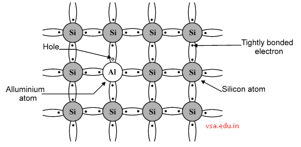
All these elements are trivalent. Each atom has 3 valence electrons. When Aluminium is mixed with pure Si crystal 3 electrons of each atom are shared with 3 neighboring Si atoms to form covalent bonding. But the forth Si atom is unable to form covalent bond. So a vacancy known as hole as positive charge, is produced as shown in the following figure. This hole carries electric current by accepting one electron, and shifting from one place to another. Hence, Aluminium is known as accepter atom.
N-type semiconductor: It contains large number of negative charges i.e. electrons, known as majority charges. Hence it is called N-type semiconductor (N for negative-electrons).The doping elements are –
- Phosphorous (P) – 15: 2+8+5 valence electrons
- Arsenic (As) – 33: 2+8+18+5 valence electrons
- Antimony (Sb) – 51: 2+8+18+18+5 valence electrons
- Bismuth (Bi) – 83: 2+8+18+32+5 valence electrons
All these elements are pentavalent. Each atom has 5 valence electrons. When Arsenic is mixed with pure Si crystal, 4 out of 5 electrons of each atom are shared with 4neighboring Si atoms to form covalent bonding. One electron becomes extra electron.
It is a free electron, as shown below. This electron can carry electric current through the material. Hence, Arsenic is known as donor atom.
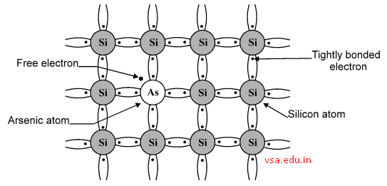
In both P-type and N-type, thermally generated hole-electron pairs are produced due to external heat. So in P-type there are electrons as minority charges and in N-type there are holes as minority charges.
Comparison of P-type and N-type semiconductor
P-type semiconductor
- Trivalent element used for doping
- Positive charges i.e. hole in majority
- Negative charges i.e. electrons in minority
- Holes in P-type accept electrons from outside, hence, known as accepter atoms.
- Impurity elements are Aluminium, Gallium, Indium and Boron
- Holes are responsible to carry electric current.
- Thermally generated hole-electron pairs are produced in both P-type and N-type.
N-type semiconductor
- Pentavalent element used for doping
- Negative charges i.e. electrons in majority
- Positive charges i.e. hole in minority
- Electrons are extra in N-type, which are donated to holes, hence, known as donor atoms.
- Impurity elements are Bismuth, Arsenic, Antimony and Phosphorous.
- Electrons are responsible to carry electric current.
- Thermally generated hole-electron pairs are produced in both P-type and N-type.
