- What is Conductor, insulator & semiconductor?
- What is Intrinsic Semiconductor?
- What is Extrinsic Semiconductor?
- Crystal Structure & Behavior of semiconductor
- Comparative Analysis of Energy Level Diagrams
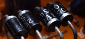
- Construction of PN junction diode
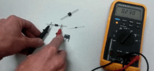
- How to find out the anode & cathode of a diode using a multimeter?
- What is Forward & Reverse Biasing of PN Junction?
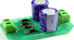
- Rectifier Circuits: HWR, FWR & BR
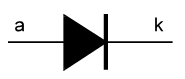
A PN junction diode is the first semiconductor device in semiconductor family. It is also known as unidirectional current device, because it allows current only in one direction through it.
When P-layer and N-layer are joined together, as shown in following figure, the PN junction is formed. Its internal structure is given below.
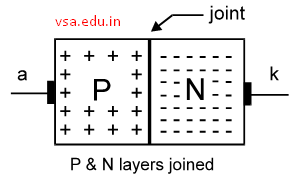
(this diagram is only for understanding)
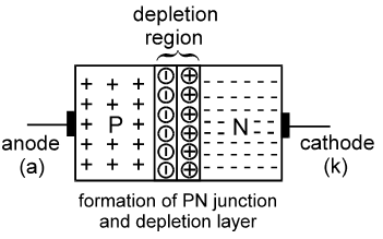
When the layers are joined, the Arsenic atoms near the junction donate their fifth electron to the nearest Aluminium atoms in P-layer. Due to this exchange of charges, Arsenic atoms loose one electron and become positive ions (+). At the same time, Aluminium atoms accept one electron from Arsenic. So they become negative ions (-). Thus opposite types of charges are produced across the junction, as shown above.
These ions oppose further flow of electrons from N-layer to P-layer. The process of charge exchange stops automatically. This opposing force of ions across the junction is called potential barrier.
The area where these ions are present is known as depletion layer. For Silicon diode, the potential of this barrier is 0.6 to 0.7V and for Germanium it is 0.2 to 0.3V.
Introduction to PN Junction Diode
The PN junction diode is a fundamental electronic component in semiconductor technology. It is a two-terminal device that allows current to flow in one direction while blocking it in the other. This article explores its history, scientific contributions, and functionality in detail.
Historical Background
The PN junction diode was discovered by Russell Ohl in 1939. His work laid the foundation for modern semiconductor devices. Before the PN junction, rectification properties were observed in metal semiconductor contacts, but Ohl’s discovery marked a significant advancement. Over the years, enhancements in diode technology, such as the development of Schottky and tunnel diodes, have expanded its applications.
Basics of Doping and Semiconductor Properties
Semiconductors like silicon and germanium are doped with impurities to create p-type and n-type materials. Doping involves adding elements such as boron (for p-type) and phosphorus (for n-type) to alter the electrical properties. This process increases the number of charge carriers, enabling the creation of a PN junction.
Formation of the PN Junction
When p-type and n-type materials are joined, electrons from the n-region diffuse into the p-region, and holes from the p-region diffuse into the n-region. This movement creates a depletion region, devoid of free carriers, and an electric field forms to counteract further diffusion.
Depletion Region and Potential Barrier
The depletion region forms due to the recombination of electrons and holes near the junction. This region is characterized by immobile ionized atoms that create an electric field, leading to a potential barrier. This barrier prevents further movement of carriers across the junction under equilibrium conditions.
Biasing the PN Junction
The PN junction can be biased in two ways:Forward Bias: Applying a positive voltage to the p-region reduces the potential barrier, allowing current to flow. The VI characteristics exhibit exponential growth in current beyond the threshold voltage, also called the knee voltage.Reverse Bias: Applying a positive voltage to the n-region increases the potential barrier, preventing current flow. However, a small leakage current exists due to minority carriers.
VI Characteristics
The VI characteristics of a PN junction diode illustrate its behavior under different biasing conditions. In forward bias, the current increases exponentially after crossing the knee voltage, typically 0.7V for silicon diodes. In reverse bias, the current remains negligible until breakdown occurs at high reverse voltages.
Types of Diodes
There are various types of diodes, each designed for specific applications:
- Rectifier Diodes: Used in AC to DC conversion.
- Zener Diodes: Operate in reverse bias for voltage regulation.
- Light Emitting Diodes (LEDs): Emit light when forward biased.
- Photodiodes: Generate current when exposed to light.
Applications of PN Junction Diode
PN junction diodes are widely used in:
- Rectification of AC to DC.
- Signal demodulation.
- Voltage regulation.
- Display and lighting (LEDs).
Energy Band Structures of p-Type and n-Type Semiconductors
Semiconductors are categorized into p-type and n-type based on the type of majority charge carriers present.
- n-Type Semiconductor: When a pure silicon or germanium crystal is doped with pentavalent elements (e.g., phosphorus or arsenic), extra electrons are introduced into the lattice. These extra electrons occupy energy levels just below the conduction band, known as the donor energy level. The conduction band is only slightly higher in energy, making it easy for electrons to move into it and conduct electricity.
- p-Type Semiconductor: When the crystal is doped with trivalent elements (e.g., boron or aluminum), a shortage of electrons creates “holes” in the valence band. These holes act as positive charge carriers. The acceptor energy level is created slightly above the valence band.
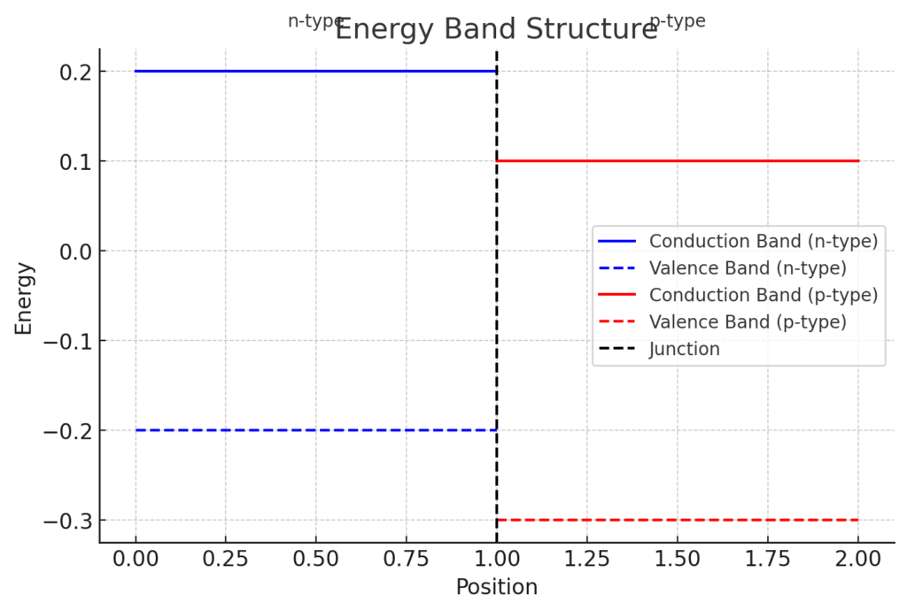
Refer to the Energy Band Structure diagram to observe the energy levels of conduction and valence bands for both n-type and p-type materials, along with the junction separating the two regions.
Formation of the Depletion Region
When a p-type material is joined to an n-type material, the following occurs:
- Diffusion of Charge Carriers: Electrons from the n-region move to the p-region, filling the holes. Similarly, holes from the p-region diffuse into the n-region.
- Recombination: As electrons and holes recombine near the junction, the region becomes devoid of free charge carriers.
- Depletion Region: The immobile, ionized donor atoms in the n-region and acceptor atoms in the p-region create an electric field. This field opposes further diffusion of charge carriers, forming a depletion region.
- Potential Barrier: The electric field gives rise to a potential difference across the junction, known as the potential barrier, which prevents further movement of electrons and holes under equilibrium.
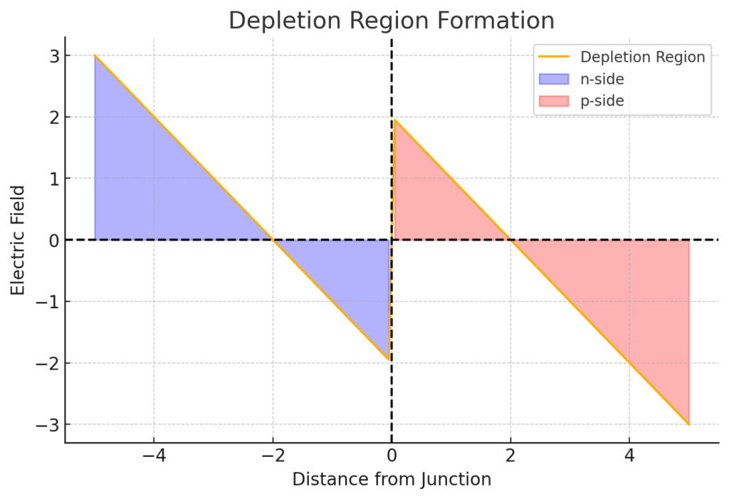
The Depletion Region Formation diagram illustrates the electric field and the regions of immobile ions in both the p- and n-sides.
VI Characteristics Curve
The voltage-current relationship of a PN junction diode can be categorized into two regions based on biasing:
Forward Bias
- When a positive voltage is applied to the p-side, the potential barrier reduces, allowing charge carriers to flow across the junction.
- The current remains negligible below a certain threshold, known as the knee voltage (typically 0.7V for silicon diodes). Beyond this voltage, the current increases exponentially.
Reverse Bias
- When a positive voltage is applied to the n-side, the potential barrier increases, and only a small leakage current flows due to minority carriers.
- If the reverse voltage exceeds the breakdown voltage, a significant current flows, potentially damaging the diode if uncontrolled.
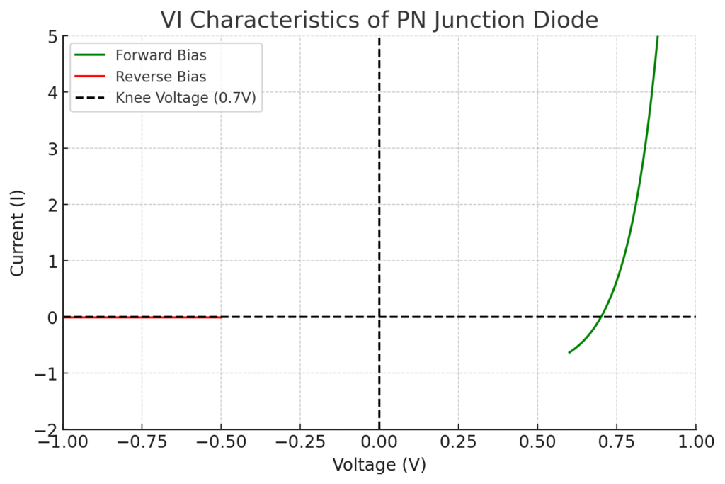
The VI Characteristics diagram shows the exponential current rise in forward bias and the negligible current in reverse bias until breakdown.
Carrier Movement under Forward and Reverse Bias
Forward Bias
- In forward bias, the applied voltage reduces the potential barrier.
- Electrons in the n-region gain enough energy to cross the junction and recombine with holes in the p-region.
- Simultaneously, holes move from the p-region to the n-region, facilitating continuous current flow.
Reverse Bias
- In reverse bias, the potential barrier increases, preventing the majority carriers from crossing the junction.
- A small leakage current occurs due to the movement of minority carriers. Electrons from the p-region move toward the n-region, and holes from the n-region move toward the p-region.
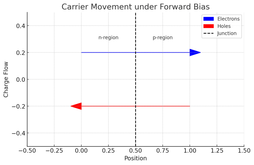
Refer to the Carrier Movement under Forward Bias diagram for a visualization of how electrons and holes move in forward bias conditions.