- What is Conductor, insulator & semiconductor?
- What is Intrinsic Semiconductor?
- What is Extrinsic Semiconductor?
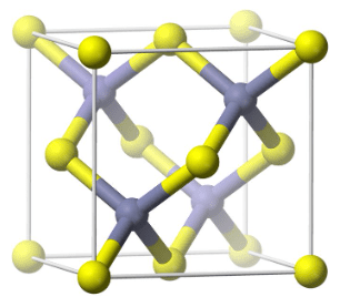
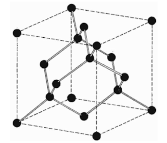
- Crystal Structure & Behavior of semiconductor
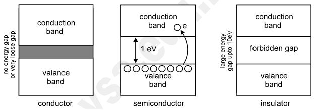
- Comparative Analysis of Energy Level Diagrams
- Construction of PN junction diode
- How to find out the anode & cathode of a diode using a multimeter?
- What is Forward & Reverse Biasing of PN Junction?
- Rectifier Circuits: HWR, FWR & BR
At temperatures above absolute zero, some electrons are excited out over the band gap into the conduction band. When the electron in pure silicon crosses the gap, it creates a vacancy, known as a hole, in the regular silicon lattice. A hole means actually nothing. But since it can accept an electron to get occupied into it, it is assumed to have a positive charge. This is also assumed to be a thing, as we want two types of charges for their distinction: the positive and the negative charges, in order to understand the current conduction behavior in semiconductor.
Now under the influence of sufficient external voltage, both the electron and the hole can move through the material. Thus at room temperatures and somewhat above, the current which will flow in an intrinsic semiconductor consists of both electron and hole current. That is, the electrons which have been freed from their lattice positions into the conduction band can move through the material. Also, other electrons move within the lattice positions to fill the vacancies produced by escaped electrons. This supplementary mechanism is called as conduction due to holes, because the holes are virtually migrating across the material, in the direction opposite to the flow of free electrons.
It thus appears that pure Silicon at room temperature is a nice semiconductor material, which can be directly used in electronic circuits. But it has a peculiar disadvantage. And that is, the current flowing through it, by both holes and electrons is temperature dependent. A small variation in temperature causes uncontrollable transitions in this current. Hence, it is not suitable to directly implement in electronic circuit, as the energy required to break conduction bands is just about 1.12eV for Si and 0.75eV for Ge!
Energy Levels
According to Bohr’s atomic model1, an atom consists of positively charged nucleus around which negatively charged electrons revolve in different circular orbits. These electrons can revolve in certain permitted orbits, having certain fixed radii. They have fixed amount of energy. Thus larger is the orbit, i.e. r2 > r1, greater is the amount of energy.
However, if an electron is provided with additional energy in terms of heat, light, etc. then it is lifted to higher orbit. In this case, we say that the atom is in state of excitation. This is a transient state and soon ends up, as the electron falls back to lower orbit. While falling back it gives out energy in the form of radiation.
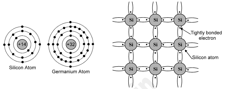
Now for Silicon, it has 14 electrons with specific arrangement, as discussed in section above. These orbits are known as K, L, M orbits, respectively. The simple way of representing the energy of different orbits is given in following Figure. In terms of energy band, the valence band is almost filled with electrons and the conduction band is almost empty i.e. deficient of electrons. Also the energy gap between valence band and conduction band is far less than insulators.
So with the application of small about of electric field, (of course, greater than insulators) is required to push the electrons from valence band into conduction band. Thus at smaller temperature, the semiconductor behaves almost like an insulator. And as the temperature increases, almost at room temperature, the electrons start crossing the energy gap and get pushed into conduction band2. Hence, it is certain that the semiconductor shows the property of negative temperature coefficient of resistance.
1. The Rutherford–Bohr model of the hydrogen atom (Z = 1) or a hydrogen-like ion (Z > 1), where the negatively charged electron confined to an atomic shell encircles a small, positively charged atomic nucleus and where an electron jump between orbits is accompanied by an emitted or absorbed amount of electromagnetic energy (hν).
2. Nearly about a single electron is pushed into conduction band, out of 1010 atoms present in valence band.