- What is Conductor, insulator & semiconductor?
- What is Intrinsic Semiconductor?
- What is Extrinsic Semiconductor?
- Crystal Structure & Behavior of semiconductor
- Comparative Analysis of Energy Level Diagrams
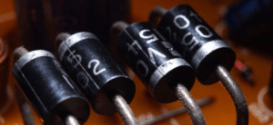
- Construction of PN junction diode
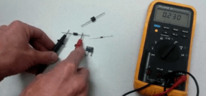
- How to find out the anode & cathode of a diode using a multimeter?
- What is Forward & Reverse Biasing of PN Junction?
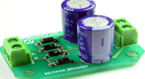
- Rectifier Circuits: HWR, FWR & BR
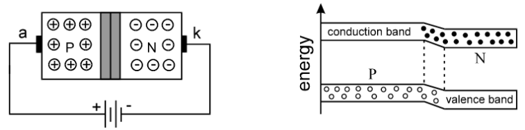
The PN junction diode conducts only in one direction. So it is known as unidirectional current device. Before going to understand the energy level diagrams, please read construction and biasing of diode.
Forward characteristics
In forward biasing of diode, free electrons from N-layer cross the junction and come into P-layer. Then they recombine with holes and then attracted by positive terminal of battery. Thus –
- In N-layer free electrons travel in conduction band.
- When they cross the junction and come into P-layer, they occupy holes.
- So from one hole to another, they travel through P-layer in valence band.
- They come out of diode and flow through the wires in conduction band and come back.
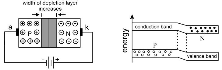
Reverse characteristics
In reverse biasing, free electrons in N-layer go away from the junction. So they produce more positive ions near the junction.
Similarly, more negative ions are produced near the junction, in P-layer. Thus, total width of depletion layer increases. So in reverse bias, electrons in conduction band and holes in valence band go away from the junction, as shown energy level diagram. Hence, potential barrier increases, till it becomes equal to battery voltage.
Why silicon diode is superior to germanium diode?
There are several reasons silicon diode is preferred over germanium diode, as follows:
- Easy formation of SiO2 or Silicon-di-Oxide layer in silicon than germanium, during the manufacturing of advanced electronic devices like MOSFETs, etc.
- Silicon is largely found in sand and so it is very cheap as compared to germanium. Germanium is generally found in the form of different compounds due to its high reactivity.
- Silicon has large band gap 1.12eV than germanium 0.7eV i.e. electron volt. So, at same temperature, the thermal pair generation in silicon is less than germanium. That is the germanium diode is more sensitive to variations in temperature as compared to silicon diode. This is because, the 4 valence electrons in germanium atom are far away than the silicon atom. So the germanium valence electrons can escape into conduction band at less temperature and increase unnecessarily the conductivity (in Mho) of the device.
- However, the germanium diode has one major advantage over Si. Ge has higher electron and hole mobility and because of this Ge devices can function up to a higher frequency than Si devices.
- On the contrary, the germanium diode is also superior to silicon diode in terms of energy loss, current loss, etc. The Ge diode loses only 0.3V to 0.4V while a silicon diode loses about 0.6V to 0.7V. But, the cost of production and non-versatility of germanium diode, makes it poor than silicon diode.