- What is Conductor, insulator & semiconductor?
- What is Intrinsic Semiconductor?
- What is Extrinsic Semiconductor?
- Crystal Structure & Behavior of semiconductor
- Comparative Analysis of Energy Level Diagrams
- Construction of PN junction diode
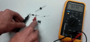
- How to find out the anode & cathode of a diode using a multimeter?
- What is Forward & Reverse Biasing of PN Junction?
- Rectifier Circuits: HWR, FWR & BR
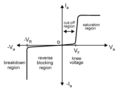
In a general meaning, the biasing means connecting a PN junction across the battery or a power supply, in forward or reverse direction.
Forward Biasing
When the external voltage applied to the PN junction is in such a direction that it cancels the potential barrier, thus permitting current flow, is called as forward biasing.
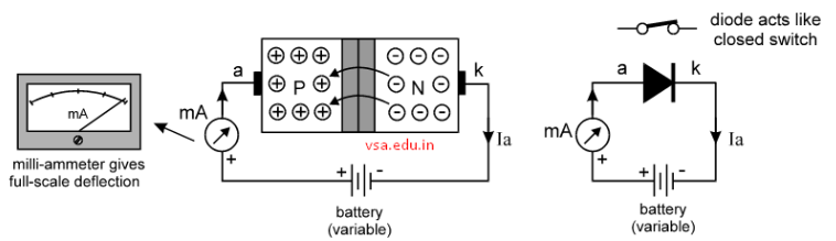
The electrons from N–layer are repelled by negative terminal of battery. So they cross the potential barrier, because the battery voltage is greater than or equal to 0.7V. These electrons enter into P–layer and some of them occupy the holes and then flow towards the +ve terminal of the battery. Then they flow through battery and come back to N-layer to complete the circuit.
When electrons flow from N–layer to P–layer and fill up holes, the holes virtually move from P–layer to N–layer. Thus electrons flow in opposite direction of conventional current but holes flow in same direction. Thus the diode provides low resistance path and large current flows through it.
Reverse Biasing
When the external voltage applied to the PN junction is in such a direction that the potential barrier is increased, it is called as reverse biasing.
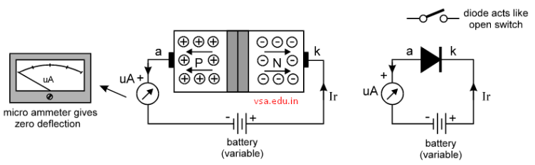
Since the battery is connected in reverse, (anode is negative and cathode is positive) the free electrons in N–layer and holes in P–layer are grouped away from the junction. The movement of majority charges from N-layer to P-layer stops. Thus, the width of depletion layer increases.
This width goes on increasing until the potential of potential barrier becomes equal to the battery voltage. If the battery voltage is further increased, the diode breaks down and large current flows through it.
This is called breakdown of diode. However, experimentally it is found that before breakdown some current flows through the diode. This current is due to minority charges called leakage current.
Characteristics Graph