- Parameters of Bipolar Transistor
- Common Collector Configuration: CC Mode
- Common Emitter Configuration: CE Mode
- Common Base Configuration: CB Mode
- How NPN transistor works? Tutorials of forward & reverse biasing of an NPN transistor
- How PNP Transistor Works?
Let us know first what is a transistor? If you are already familiar with it, skip to next topic, below.
What is transistor?
Transistor is a semiconductor device having three layers, three terminals and two junctions. Since we have only two types of semiconductors i.e. the p-type and n-type, there are two types of transistors: they are NPN transistor and PNP transistor.
It is named as transistor which is an acronym of two terms: “transfer-of-resistor.” It means that the internal resistance of transistor transfers from one value to another values depending on the biasing voltage applied to the transistor. Thus it is called TRANSfer resISTOR: i.e. TRANSISTOR.
Bipolar Transistor
A bipolar transistor is a semiconductor device in which electric current flows due to electrons and holes BOTH, simultaneously. Thus both types of charges take part in the conduction of current through it. Hence it is called bipolar transistor. There are two types of bipolar transistors, NPN and PNP transistor.
NPN Transistor
It uses three semiconductor layers: two n-type layers and one p-type layer. The p-layer is sandwiched between two n-layers, as shown below.
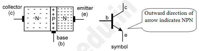
Important Points about NPN Transistor
- The area of collector layer is largest. So it can dissipate heat quickly.
- Area of base layer is smallest and it is very thin layer.
- Area of emitter layer is medium.
- Collector layer is moderately doped. So it has medium number of charges (electrons).
- Base layer is lightly doped. So it has a very few number of charges (holes).
- Emitter layer is heavily doped. So it has largest number of charges (electrons).
- There are two junctions in this transistor – junction J-1 and junction J-2.
- The junction between collector layer and base layer is called as collector-base junction
or c-b junction. - The junction between base layer and emitter layer is called as base-emitter junction
or b-e junction. - The two junctions have the same potential barrier voltage of 0.6V to 0.7V, just like in a diode.
Concept of Transistor Biasing
When external voltage is applied to the junction of transistor in such a direction that it cancels out the potential barrier, so that electric current flows through it, is called as transistor biasing.
Now to obtain easy current flow through the transistor it must be biased by connecting external batteries. So there must be two batteries to apply proper bias across the two junctions of the transistor.
For example, the NPN transistor can be biased using three different methods –
FF biasing: In this method both the junctions are forward biased. For this, two external batteries are connected across two junctions such that collector is negative w.r.t. base and base is positive w.r.t. emitter. This method is not useful as the transistor is in “saturation” and the current cannot be controlled easily.
RR biasing: In this method both the junctions are reverse biased. For this, two external batteries are connected across two junctions such that collector is positive w.r.t. base& base is negative w.r.t. emitter. This method is also not useful as the transistor is in “cut-off” state since current is zero.
FR biasing: This is the most common and popular method used in transistor biasing. In this method, the base-emitter junction is forward biased and collector-base junction is reverse biased.
For this, two external batteries are connected across two junctions such that collector is positive w.r.t. base and base is positive w.r.t. emitter. So by adjusting base voltage we can control total current in the transistor easily.
Forward Biasing of NPN Transistor
The NPN transistor can be used in two different modes: forward biased mode and the reverse biased mode. In forward biased mode, the electric current can easily flow through it. So it acts like a CLOSED SWITCH. However, in reverse biased mode, the current through it is practically zero and thus, it acts like an OPEN SWITCH.
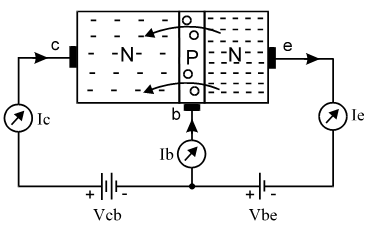
To forward bias an NPN transistor it is connected as shown in the above circuit. Read following points to understand the process easily –
- The collector is connected to high positive voltage with respect to base i.e. Vcb is very high. So c-b junction is reverse biased. Vcb >> Vbe.
- The base is connected to low positive voltage with respect to emitter i.e. Vbe is low.
- When we increase Vbe 0.7V (potential barrier voltage) the transistor is forward biased.
- Now large number of electrons in emitter layer is repelled by negative terminal of Vbe and they flow towards b-e junction.
- They cross the junction and enter into small base layer. Here some electrons combine with holes. Also some of them are attracted by positive terminal of Vbe and remaining maximum number of electrons flow into collector layer, crossing the second junction i.e. c-b junction.
- The resident electrons of collector are repelled by these (guest) electrons and thus, all the electrons are attracted by positive terminal of Vcb.
- Thus, all these electrons complete their journey back into emitter layer and thus, produce conventional currents in the transistor as shown in the above circuit.
- Thus, as per Kirchhoff Current Law, we can write: Ic + Ib = Ie
- Now when Vbe is still increased, more electrons are repelled by negative terminal of Vbe. So base-emitter junction is more and more forward biased. Thus the base current (Ib) increases.
- Hence, we can say that collector current (Ic) is the function of base current (Ib).
- So collector current is directly proportional to the base current i.e. Ic ∝ Ib.
- Maximum number of electrons from emitter layer flow into collector layer. So collector current is ALMOST EQUAL to emitter current, i.e. Ic ≈ Ie.
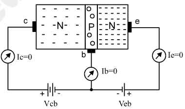
Reverse Biasing of NPN Transistor
In this method both the junctions are reverse biased as the batteries are connected in opposite direction as shown in the adjacent diagram. The Vcb battery reverse biases CB junction. Similarly, the Veb battery reverse biases BE junction. So charges cannot flow and current in the transistor is practically zero.