- IC 555 Bible: Everything About It!
- IC 555 FAQs
- Real Time Simulation of IC 555 Working using Block Diagram
This is the laboratory tested real time simulation of Internal Block diagram working of IC 555. First read the following part and then watch the video given on my YouTube channel so that you will understand the working of the IC very easily and systematically.
In this IC, two comparators, one RS flip flop, one discharging transistor, and three resistors are used.
Observe the internal connectivity of different components given in the following diagram and understand functioning of 8 pins of this IC. And then read the basic concept of working of IC and finally watch the video.
Features
- It is a very popular timer IC. It is widely used in different electronic circuits like timer, oscillator, etc. It produces very accurate time delay with three different types: ON delay timer, OFF delay timer and the Periodic timer.
- Low cost timer IC.
- It can be used as ON delay timer & OFF delay timer (monostable multivibrator) and periodic timer (astable multivibrator).
- It provides complementary output i.e. its output can sink and source current of about 200mA. For example, when output is high i.e. positive (binary-1), then it gives out the output current. When output is low i.e. negative (binary-0), then it absorbs the current at its output from outside.
- It produces accurate time delay and it is independent of battery voltage. For example, if the IC has delay of 5 seconds on 10V battery supply, then same delay will be obtained on 5V, 12V, etc.
- The IC can work on wide range of battery voltage from 3V to 18V.
- It is compatible with digital circuits i.e. logic gates circuits.
- It is available in DIL and metallic packages.
- Its output frequency is very high.
- It can be used in advanced applications like modulation and flip-flop (bi-stable multivibrator).
Pin Configuration
The pin-wise function of the eight pins of the IC is given below. These functions are applicable to all types of IC 555 timer.
- Pin-1: It is the ground pin of the IC.
- Pin-2: It triggers i.e. starts the timing cycle of the IC. When it receives 1/3 of battery voltage for a short time, it triggers the IC. When IC is triggered, its output becomes HIGH and pin-7 becomes OFF.
- Pin-3: This is the output pin of the IC. It can SINK or SOURCE a maximum current of 200mA.
- Pin-4: It resets the timing cycle of the IC. When we don’t want to reset the IC, this pin must be connected to positive terminal of battery.
- Pin-5: This pin is called control voltage pin. We can apply variable voltage like triangular wave to this pin to modulate the output waveform of the IC. This pin is useful in advanced applications of modulation.
- Pin-6: It is the threshold pin. When it receives 2/3 of battery voltage, it stops the timing cycle of the IC. When time cycle stops, output of the IC becomes LOW and pin-7 turns ON.
- Pin-7: It is the discharge pin. It discharges external capacitor (known as timing capacitor) into it.
- Pin-8: Positive supply pin. The supply voltage range of the IC is from 3V to 18V DC.
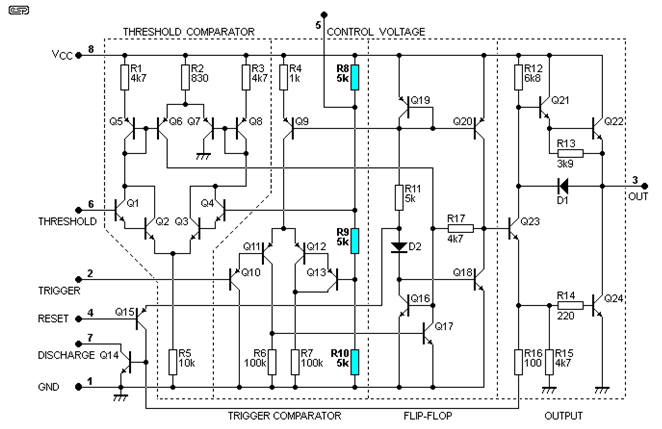
Internal block diagram
The internal block diagram of IC 555 is given below. It works on DC power supply from 3V to 18V. It has four main sections, as explained below.
5kΩ Potential divider: There are three 5kW resistors connected in series and parallel with the battery supply. They divide the supply voltage in three EQUAL parts i.e. 1/3 of supply voltage.
The comparators: There are two types of comparators used in the IC. When pin-2 receives 1/3 of battery voltage, the trigger comparator RESETs the RS Flip flop. So output at pin-3 becomes HIGH and pin-7 is cut off internally. When pin-6 receives 2/3 of battery voltage, the threshold comparator SETs the RS Flip flop. So output at pin-3 becomes LOW and pin-7 becomes active and starts discharging timing capacitor into it.
RS Flip Flop: It is a simple circuit of set-reset flip flop i.e. RS flip flop. When IC is triggered it is RESET and when timing cycle stops, the flip flop is SET.
Discharge transistor: When IC is triggered, the RS flip flop is RESET. So its output and . So internal transistor becomes OFF, pin-7 is cut off and pin-3 becomes HIGH.
But when pin-6 receives 2/3 of battery voltage, the RS flip flop is SET. So output and . So transistor becomes ON and pin-7 starts discharging the external timing capacitor.
Simulation Video
Watch the video of simulation created in Circuit Wizard Student Edition Software.