- IC 555 Bible: Everything About It!
- IC 555 FAQs
- Real Time Simulation of IC 555 Working using Block Diagram
IC 555 Bible contains complete details about the IC. The IC is perhaps the most popular IC in the history of electronics. How IC555 timer works is really interesting to study. In the following paragraphs you will learn everything about IC555.
Introduction
IC 555 timer is a highly stable integrated circuit. It can function as an accurate time delay generator and free running multivibrator as well. When it is used as an oscillator, its frequency and duty cycle can be accurately adjusted with the help of external components like resistors and a capacitor. The IC has also the facility to trigger and reset on the falling edges of waveforms. Its salient features are as follows:
Silent Features
- It can provide timing from microseconds through hours.
- It can be used as Monostable, Astable and Bistable Multivibrator
- Its duty cycle can be adjusted very accurately.
- It can work on wide range of supply voltages from 3V to 18V DC.
- Its output is compatible with CMOS, DTL and TTL logics.
- It can provide high current sink or source output of 200mA
- It has a separate trigger and reset input terminals.
- Its output can be operated as normal ON and normal OFF conditions.
- Last but not the least, it has high temperature stability.
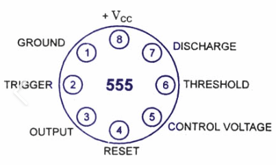
Pinout Diagram
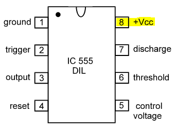
(Note highlighted pin-8, its +ve supply pin)
- Pin-1: It is the ground pin of the IC.
- Pin-2: It triggers i.e. starts the timing cycle of the IC. When it receives 1/3 of battery voltage for a short time, it triggers the IC. When IC is triggered, its output becomes HIGH and pin-7 becomes OFF.
- Pin-3: This is the output pin of the IC. It can SINK or SOURCE a maximum current of 200mA.
- Pin-4: It resets the timing cycle of the IC. When we don’t want to reset the IC, this pin must be connected to positive terminal of battery.
- Pin-5: This pin is called control voltage pin. We can apply variable voltage like triangular wave to this pin to modulate the output waveform of the IC. This pin is useful in advanced applications of modulation.
- Pin-6: It is the threshold pin. When it receives 2/3 of battery voltage, it stops the timing cycle of the IC. When time cycle stops, output of the IC becomes LOW and pin-7 turns ON.
- Pin-7: It is the discharge pin. It discharges external capacitor (known as timing capacitor) into it.
- Pin-8: Positive supply pin. The supply voltage range of the IC is from 3V to 18V DC.
The above pin-wise functions are applicable to all types of IC 555 timer.
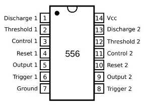
Package Type
IC555 is available in 8-pin and 14-pin dual-in-line packages and also in circular TO-99 package. The TO-99 package is a metal can package with 8 metal leads.

The SE & NE Versions
The SE and NE versions are similar except for maximum temperature ratings. The precision type SE has a large temperature range from -55°C to +125°C. The NE version is a general purpose type version. Its temperature range is from 0°C to +70°C.
Some manufacturers use the suffix C to indicate the commercial version of this general purpose version for ordinary applications.
Operating Voltage & Power Dissipation
Both these types can be operated on a wide range of supply voltage from 3V to 18V DC with a maximum power dissipation of up to 600mW.
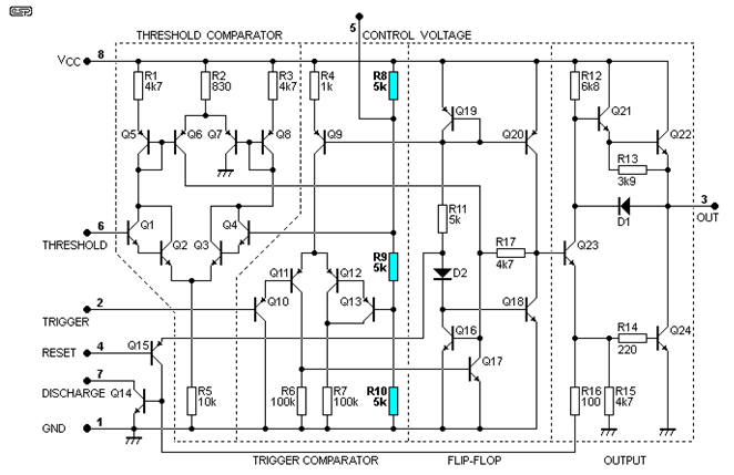
Internal Block Diagram
The internal block diagram of IC 555 is given below. It works on DC power supply from 3V to 18V. It has four main sections, as explained below.

(Applicable to all versions of IC555)
The 5K Resistors Potential Divider
There are three 5kΩ resistors connected in series and parallel with the battery supply. They divide the supply voltage in three EQUAL parts i.e. 1/3 of supply voltage.
The Comparator
A Comparator is a circuit particularly built using opamp, to compare two different voltage values. There are two types of comparators used in IC555 – the threshold comparator and the trigger comparator. The output of both these comparators is connected to RS Flipflop. The output of threshold comparator is connected to SET pin and output of trigger comparator is connected to RESET pin of RS Flipflop, as shown in above block diagram.
These two comparator SETs or RESETs the RS Flipflop and thus toggling action takes place at the output pin-3 of IC555.
When pin-2 receives 1/3 of battery voltage, the trigger comparator RESETs the RS Flip flop. So output at pin-3 becomes HIGH and pin-7 is cut off internally. When pin-6 receives 2/3 of battery voltage, the threshold comparator SETs the RS Flip flop. So output at pin-3 becomes LOW and pin-7 becomes active and starts discharging timing capacitor into it.
RS Flip Flop
It is a simple circuit of set-reset flip flop i.e. RS flip flop. When IC is triggered it is RESET and when timing cycle stops, the flip flop is SET.
Discharge transistor
When IC is triggered, the RS flip flop is RESET. So its output Q = 0 and Q ̅ = 1. So internal transistor T1 becomes OFF, pin-7 is cut off and pin-3 becomes HIGH. But when pin-6 receives 2/3 of battery voltage, the RS flip flop is SET. So output Q = 1 and Q ̅= 0. So transistor T1 becomes ON and pin-7 starts discharging the external timing capacitor.
Animated Block Diagram Working
Full Internal Circuit
The IC is designed very intelligently. It contains 23 transistors, 2 diodes and 16 resistors. The IC has built-in compensation for component tolerance and temperature drift resulting in a temperature coefficient of only 25 parts/million/°C.
Operation of IC555
Now we shall see details of operation of the IC like feeding the load, driving a relay, triggering techniques, resetting the IC, use of control voltage terminal, etc.
Feeding the load
If you observe the full internal Circuit of IC555, as given above, in the output circuitry of IC555 you will see that there are two transistors, Q22 and Q24. These two transistors are arranged in Quasi-complementary transformer-less arrangement. In this type of arrangement, one side of the load goes to the emitter-collector junction of output transistors and other side of the load can be connected to either +ve or -ve terminal of power supply. So this is also allowed in the working circuits of IC555. Thus you can connect pin-3 of the IC either to sink or source the load current.
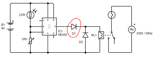
How to drive relay?
To drive a relay using IC555 is rather tricky! If you connect the relay coil directly between pin-3 of the IC and ground, the relay will remain always ON. Also you must note that when you are using a relay in the output of the IC, the time delay or time interval must be longer than 0.1 second. It is always a good practice to connect a reverse biased diode across the relay coil to absorb back e.m.f. within coil in order to avoid damage to the IC.
Source Current Drive
When you connect a relay coil between pin-3 and ground, you must connect a diode in series with the relay coil, as shown below. Otherwise a voltage equal to one diode junction drop (about 0.7V) will appear at pin-3 and it will lock the output of the IC.
Sink Current Drive
When you connect the relay coil between +ve terminal of supply and pin-3 of the IC, then only one diode in anti-parallel condition across the relay coil, is recommended. Connect the relay as shown below, so that when the output of the IC goes LOW, the relay will be activated and when output is HIGH, the relay will be OFF.

Triggering Techniques
Since the IC is generally used as a timer, it can be triggered as per requirement. The simplest method of triggering the IC is to momentarily ground pin-2. But it is necessary that its ground contact must be removed before the end of the time interval. Also it is very important to note that when IC is triggered, the circuit becomes immune to further triggering until the cycle is completed. The triggering voltage for the IC ranges from 1.67V when supply voltage is 5V to 5V when supply voltage is 15V. The triggering current required is about 0.5uA for a period of 0.1uS. These parameters are practically tested in Vidyasagar Academy Lab.
The interesting thing about triggering of the IC is that if the trigger pin-2 is floating and you just touch pin-2, the IC will be triggered as shown in the following circuit.

Resetting Techniques
As said earlier, that when IC is triggered, the circuit becomes immune to further triggering until the cycle is completed. But this triggering event can be interrupted by grounding the reset pin-4 of the IC. You can also apply a short -ve going pulse to pin-4 to reset the IC.
When the IC is reset, the timing capacitor starts discharging and the output of the IC at pin-3 becomes LOW. The reset voltage is typically 0.7V and the reset current is about 0.1mA.
Lab Note: When reset terminal is not in use, always connect it to +ve terminal of power supply.
We can use the reset pin in different interesting applications. One such practically tested circuit of Infrared Burglar Alarm is given on this link: https://youtu.be/oEghKKn7-gw
Control Voltage Pin-5
If you observe the block diagram of DC you will see that pin-5 is connected at the top part of the 5k resistor ladder. It means that the reference voltage of Threshold comparator will be ⅔ of the supply voltage.
So the timing cycle can be modified by applying a DC control voltage to pin-5 of the IC. This provides the facility of manual or electronic remote control of the time interval of the IC555.
This pin of the IC is rarely used when timer is operated in monostable mode and it should be grounded through 0.01uF capacitor. This helps to prevent the time interval from being affected by pickup of a stray AC or RF signals. Also when the timer IC is operated in Astable multivibrator mode i.e. oscillator mode, the generated signal can be frequency modulated or pulse width modulated by applying a variable DC control voltage to pin-5 of the IC.
General Applications
The general purpose applications of IC555 can be listed as follows. Remember, all these applications are covered in the series ALL ABOUT IC555. Some of the regular applications are listed as follows:
- Astable multivibrator, Monostable multivibrator, Bistable multivibrator
- On-delay timer, Off-delay timer
- Periodic timer
- Variable duty cycle square wave oscillator
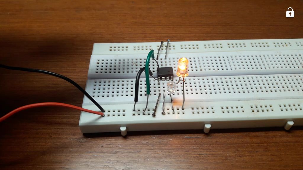
- LED flasher
- Audio tone generator