- Introduction to Bipolar & Unipolar Transistors
- Construction of Uni Junction Transistor (UJT)
- Junction Field Effect Transistor (JFET)
- Construction of MOSFET
Definition: The Unipolar transistor is a type of transistor in which electric current flows due to only one type of charges i.e. either holes or electrons.
The Unipolar transistor is categorized into two main types:
- Junction Field Effect Transistor (JFET)
- N-channel JFET
- P-channel JFET
- Metal Oxide Semiconductor Field Effect Transistor (MOSFET)
- N-channel MOSFET
- P-channel MOSFET
Construction of JFET
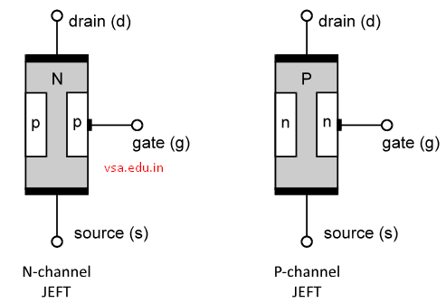
It consists of one long n-channel with two p-layers inserted at the sides. The n-channel forms the conducting path for the charges.

Note the direction of the arrow in the symbol, the inward direction of arrow indicates N-channel JFET and the outward direction of arrow indicates P-channel JFET.
We can also consider the working of JFET in terms of bipolar transistor. For this we can consider that –
- Drain (d) of JFET is similar to collector (c) in bipolar transistor.
- Source (s) of JFET is similar to emitter (e) in bipolar transistor.
- And finally, Gate (g) of JFET is similar to base (b) for bipolar transistor.
Parameters of JFET
There are three important parameters of JFET, they are as follows –
Dynamic drain resistance: It is defined as the ratio of change in the drain voltage Vds to the corresponding change in the drain current Id, at constant Vgs.
rd = ΔVds / ΔId …… at constant ΔVgs
Mutual Conductance or Transconductance: It is defined as the ratio of change in drain current Id to the corresponding change in the gate-source voltage Vgs, at constant Vds.
gm = ΔId / ΔVgs …… at constant ΔVds
Amplification factor: It is defined as the ratio of change in the drain-source voltage to the corresponding change in gate-source voltage, at constant drain current Id.
μ = ΔVds / ΔVgs …… at constant ΔId
Generally, the amplification factor is also given as –
μ = rd × gm


