
A Metal oxide semiconductor field effect transistor (MOSFET) is also known as the IGFET i.e. insulated gate FET. The schematic constructional diagrams of both n-channel and p-channel MOSFETs are given below.

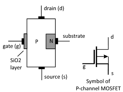
Just like JFET, an N-channel is taken and a single p-layer is inserted between the N-channel. At the left side an insulated gate is attached through SiO2 layer i.e. Silicon-di-Oxide Layer.
This SiO2 layer is very thin and small in size. Due to insulated gate, the current through it is extremely small as its is very high (theoretically, it is of the order of 10,000 MΩ to 10,000,000 MΩ).In the same way, P-channel MOSFET is manufactured.
An n-layer is inserted between the P-channel. The SiO2 layer is inserted between the gate terminal to produce insulation for the gate, so that the device becomes voltage operated device.

