- Parameters of Bipolar Transistor
- Common Collector Configuration: CC Mode
- Common Emitter Configuration: CE Mode
- Common Base Configuration: CB Mode
- How NPN transistor works? Tutorials of forward & reverse biasing of an NPN transistor
- How PNP Transistor Works?
Let us know first what is a transistor? If you are already familiar with it, skip to next topic, below.
What is transistor?
Transistor is a semiconductor device having three layers, three terminals and two junctions. Since we have only two types of semiconductors i.e. the p-type and n-type, there are two types of transistors: they are NPN transistor and PNP transistor.
It is named as transistor which is an acronym of two terms: “transfer-of-resistor.” It means that the internal resistance of transistor transfers from one value to another values depending on the biasing voltage applied to the transistor. Thus it is called TRANSfer resISTOR: i.e. TRANSISTOR.
Bipolar Transistor
A bipolar transistor is a semiconductor device in which electric current flows due to electrons and holes BOTH, simultaneously. Thus both types of charges take part in the conduction of current through it. Hence it is called bipolar transistor. There are two types of bipolar transistors, NPN and PNP transistor.
NPN Transistor
It uses three semiconductor layers: two n-type layers and one p-type layer. The p-layer is sandwiched between two n-layers, as shown below.

Important Points about NPN Transistor
- The area of collector layer is largest. So it can dissipate heat quickly.
- Area of base layer is smallest and it is very thin layer.
- Area of emitter layer is medium.
- Collector layer is moderately doped. So it has medium number of charges (electrons).
- Base layer is lightly doped. So it has a very few number of charges (holes).
- Emitter layer is heavily doped. So it has largest number of charges (electrons).
- There are two junctions in this transistor – junction J-1 and junction J-2.
- The junction between collector layer and base layer is called as collector-base junction
or c-b junction. - The junction between base layer and emitter layer is called as base-emitter junction
or b-e junction. - The two junctions have the same potential barrier voltage of 0.6V to 0.7V, just like in a diode.
Concept of Transistor Biasing
When external voltage is applied to the junction of transistor in such a direction that it cancels out the potential barrier, so that electric current flows through it, is called as transistor biasing.
Now to obtain easy current flow through the transistor it must be biased by connecting external batteries. So there must be two batteries to apply proper bias across the two junctions of the transistor.
For example, the NPN transistor can be biased using three different methods –
FF biasing: In this method both the junctions are forward biased. For this, two external batteries are connected across two junctions such that collector is negative w.r.t. base and base is positive w.r.t. emitter. This method is not useful as the transistor is in “saturation” and the current cannot be controlled easily.
RR biasing: In this method both the junctions are reverse biased. For this, two external batteries are connected across two junctions such that collector is negative w.r.t. base& base is negative w.r.t. emitter. This method is also not useful as the transistor is in “cut-off” state since current is zero.
FR biasing: This is the most common and popular method used in transistor biasing. In this method, the base-emitter junction is forward biased and collector-base junction is reverse biased.
For this, two external batteries are connected across two junctions such that collector is positive w.r.t. base and base is positive w.r.t. emitter. So by adjusting base voltage we can control total current in the transistor easily.
Forward Biasing of NPN Transistor
The NPN transistor can be used in two different modes: forward biased mode and the reverse biased mode. In forward biased mode, the electric current can easily flow through it. So it acts like a CLOSED SWITCH. However, in reverse biased mode, the current through it is practically zero and thus, it acts like an OPEN SWITCH.
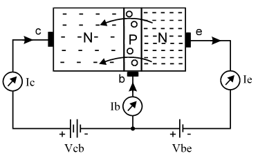
To forward bias an NPN transistor it is connected as shown in the above circuit. Read following points to understand the process easily –
- The collector is connected to high positive voltage with respect to base i.e. Vcb is very high. So c-b junction is reverse biased. Vcb >> Vbe.
- The base is connected to low positive voltage with respect to emitter i.e. Vbe is low.
- When we increase Vbe 0.7V (potential barrier voltage) the transistor is forward biased.
- Now large number of electrons in emitter layer is repelled by negative terminal of Vbe and they flow towards b-e junction.
- They cross the junction and enter into small base layer. Here some electrons combine with holes. Also some of them are attracted by positive terminal of Vbe and remaining maximum number of electrons flow into collector layer, crossing the second junction i.e. c-b junction.
- The resident electrons of collector are repelled by these (guest) electrons and thus, all the electrons are attracted by positive terminal of Vcb.
- Thus, all these electrons complete their journey back into emitter layer and thus, produce conventional currents in the transistor as shown in the above circuit.
- Thus, as per Kirchhoff Current Law, we can write: Ic + Ib = Ie
- Now when Vbe is still increased, more electrons are repelled by negative terminal of Vbe. So base-emitter junction is more and more forward biased. Thus the base current (Ib) increases.
- Hence, we can say that collector current (Ic) is the function of base current (Ib).
- So collector current is directly proportional to the base current i.e. Ic ∝ Ib.
- Maximum number of electrons from emitter layer flow into collector layer. So collector current is ALMOST EQUAL to emitter current, i.e. Ic ≈ Ie.
Reverse Biasing of NPN Transistor
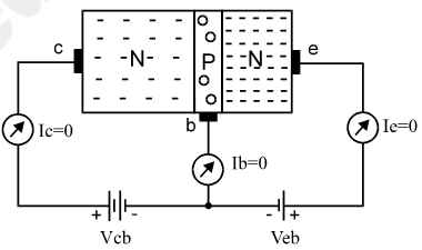
In this method both the junctions are reverse biased as the batteries are connected in opposite direction as shown in the adjacent diagram. The Vcb battery reverse biases CB junction. Similarly, the Veb battery reverse biases BE junction. So charges cannot flow and current in the transistor is practically zero.






Thank you for your blog post. Velupe and I are saving for a new e-book on this issue and your post has made us to save all of our money. Your thoughts really responded to all our queries. In fact, in excess of what we had recognized prior to when we came across your amazing blog. I no longer have doubts including a troubled mind because you have totally attended to our own needs in this article. Thanks
Nice blog
Very good and elaborated info about diffrent articles on this website.
This is a very useful website.
particularly for the students of electronics
needs a little more description
May I please know what sort of more description you need further?
Please reply, so that I can make necessary updates and enrich my website.
Thanks for visiting the site…
Points missing..How are the electrons penetrating through the reverse biased b-c junction(insulator)?
,what is the reason for small and lighted doped base(reduce time and recombination) and others too,
technically speaking transistor is dc to ac power converter.
Your queries can be explained in short as follows…
Also, I thank you for putting this query, as me too, was thinking of writing down a short note on these points in particular.
Thanks also for visiting the site.
Please don’t hesitate to point out the “points” missing…by sparing out of your valuable time….
THANKS…….
really confusing for someone who has no background
from fwd bias-> f) Now large number of electrons in emitter layer is repelled by negative terminal of Vbe and they flow towards b-e junction.
why are the electrons in emitter layer is repelled when it’s connected to negative junction of the battery which is also full of electrons??
The electrons repel each other due to mutual repulsion…like charges, as they have…
THANKS ………
Why base collector voltage >> base emiter voltage ?????
The reason that the Vcb >> Vbe, is as follows….
In the base junction negative terminal of Vcb and positive terminal of Vbe
is connected. Vcb grater then Vbe . So electrons should flow towards base .
So current should flow out of the base. ( opposite to diagram )
Then why current is flowing towards base ?
Please explain ………
I don’t understand this basic concept …..
My dear friend,
Please also read the explanation given on your next comment.
I like the way, you are asking the queries. It increases the wisdom of understanding this process in deep.
i have a doubt regarding forward bias and reverse bias connection for cc amplifier. can u plz help me out
Refer this article…
http://vsagar.com/2012/10/20/simple-details-common-collector-configuration-npn-transistor-2/
You may also refer other articles on configurations of transistor, to clear your doubts.
sir,
I have doubt when npn transistor is on or off i.e is it right if the voltage at the base is more than the emiter volage applied the transistor is on.
I would also like to know when does the transistor act as switch as well as CMOS working.
It is always the case, that when voltage across base-emitter junction of NPN transistor is greater than or equal to 0.7V, then it is forward biased.
When this voltage is quite large, say around 3V or more (upto certain limit), then total the number of free electrons in emitter layer start participating in conduction of electric current through the transistor.
This condition is called as saturation of transistor and in this condition we can use it just like a switch which is ON.
And when the base voltage is quickly reduced to zero, this process of conducting current suddenly stops and we can use the transistor just like a switch which is OFF…!
What type of CMOS info you need?
thank you for your immediate response.
sir I would like to know working of CMOSFET inverter.
Inverter is defined as the circuit that converts DC voltage source into AC voltage at required frequency.

Now CMOS-FET inverter is a device which is actually a FET (Field Effect Transistor) in CMOS technology.
CMOS-FET inverter is a simply a push-pull type FET circuit as shown below, which amplifies both halves of the AC cycle and give you reliable output of AC source.
is transistor simply means transfer of resistors? how can u say so?
Since the current through the transistor is controllable, it means that the internal resistance of the transistor is changing. The fact that when its base-emitter resistance changes it reflects the change in its collector-emitter resistance.
Hence it is termed as transfer of resistance-transistor.